The differential amplifier has the ability to suppress signals co mmon to the two inputs.
CMRR is an indicator of the ability.
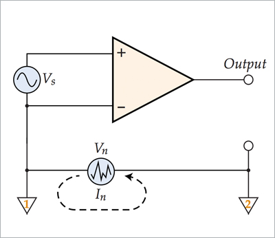
When a commercial power supply signal ( In) flows to the ground loop, a noise ( Vn) is generated and applied to the inputs of the differential amplifier as an common mode component. However, the common-mode noise component appearing at the output of the amplifier is extremely small (the common mode gain is small, ideally zero). When Adiff is the differential gain (the gain with respect to Vs in the Fig. 1) and Acom is the common mode gain (the gain with respect to Vn in the figure), CMRR is defined by the following equation.
CMRR = Adiff /Acom = Adiff [dB] – Acom [dB]

Figure1. Diagram of Differential Amplifier
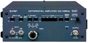
For example, NF differential amplifier 5307 CMRR is 120 dB (min.) at utility frequency. Even if 1 V is generated as the noise component Vn, only 1 μV appears at the output. As the system is larger, since the potential and impedance are different, a ground loop current flows between 1 and 2 (refer to Fig.1), then it generates noise, even though 1 and 2 look the same.

Differential Amplifier 5307
In the Actual Setup
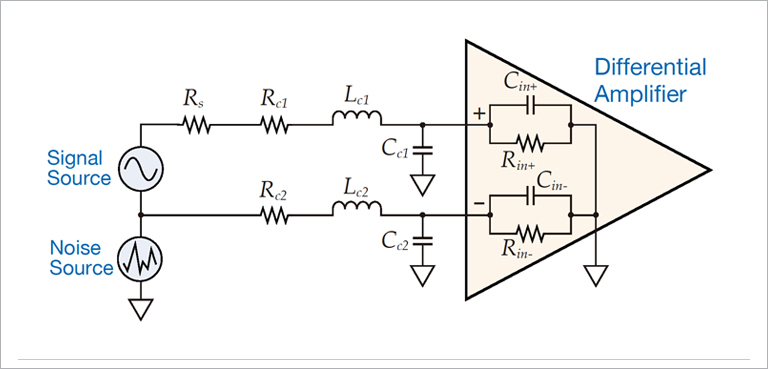
Both of the signal cable and the signal source have impedances, therefore the simplified circuit diagram in the actual use of the differential amplifier is shown as follows.
If there are no these impedances, the noise source is applied to the non inverting input terminal and the inverting input terminal of the differential amplifier with exactly the same voltage value, and there is no degradation of CMRR of the whole setup In practice, however, these values cannot be ignored, and a voltage difference will occur when the noise source is added to the non inverting and the inverting inputs terminals of the differential amplifier, which will degrade the CMRR.
For example, if the signal source impedance RS is 10 kΩ, the input resistances of the differential amplifier Rin+ and Rin- are 10 MΩ, ignoring other impedances such as Rc , the CMRR is 20 log (0.9990 / 0.0009990), which is 60.0 dB, from the differential gain: 0.9990 and the common mode gain: 0.0009990 at DC.
Next, assuming RS is 10 kΩ, CC1 + Cin+ and CC2 + Cin– are 500 pF, the differential gain is 0.9532, the common mode gain is 0.2994 at 10 kHz, and the CMRR drops to about 10.1 dB.
If there is an imbalance in the signal path between the signal source and the non inverting and inverting input terminals of the differential amplifier, we should take the CMRR degradation in account. Inserting the same impedance as RS at the non inverting input will improve CMRR.

Figure2. Equivalent Circuit Diagram
